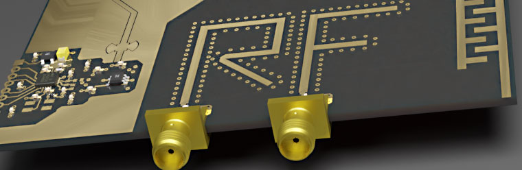
How to Optimize RF Circuit Boards for Wireless Communication
RF Circuit Boards for Wireless Communication
As the world moves to wireless communication, rf circuit board will play an increasingly important role in our lives. These high-frequency PCBs are used in devices like mobile phones, GPS, Wi-Fi and satellite systems. They require specialized materials and layouts to perform effectively in these applications. This is due to the fact that high-frequency signals travel over longer distances and are more sensitive to factors like ringing, noise and reflections. The following tips will help you optimize your RF PCB design to meet these demands.
Use specialized RF PCB materials. Choose a substrate laminate that has low losses at RF frequencies, like Rogers or PTFE. It’s also critical to consider the dielectric constant, loss tangent and coefficient of thermal expansion of these materials. This will allow you to create a board with optimized impedance characteristics, while keeping power dissipation as low as possible.
Carefully position RF components on the PCB to reduce parasitic capacitance and inductance. This will ensure that the signal path is as short as possible and minimizes signal loss. Additionally, you should utilize a multilayer PCB to minimize the number of vias and keep the board’s dimensions small.
How to Optimize RF Circuit Boards for Wireless Communication
Make sure the RF signal layer is located away from non-RF layers. This will prevent interference from interconnecting components and affecting signal quality. It is also a good idea to separate RF and analog components from digital ones. This will further improve signal integrity.
RF signals and transmission lines must match the characteristic impedance of both the source and load to avoid signal reflection and interference. Impedance matching is especially important at RF and microwave frequencies, where tolerance decreases. This can be achieved by using proper transmission line techniques, including microstrips and striplines. In addition, you should prioritize the design of your RF and microwave return paths. Ideally, the return signal should follow a ground plane to ensure maximum efficiency.
Minimize the number of buried vias in your RF PCB, as these can introduce high levels of parasitic inductance. This can lead to poor signal performance and even oscillations. Ensure that the diameter of these vias is as small as possible, and use thermal vias to manage heat generated by high-powered RF components.
Decoupling capacitors must be placed in a star configuration near the power and ground pins of all RF components. This will create a low-impedance network that will efficiently distribute power to all of the components on the board and minimize ground loops. In addition, a properly designed ground plane will eliminate unwanted interference and maintain signal integrity. Finally, you should minimize the amount of copper on the RF signal layer to keep it as thin as possible. A thicker layer will increase the parasitic inductance and cause loss of sensitivity.